- 您现在的位置:买卖IC网 > Sheet目录492 > NTMS7N03R2 (ON Semiconductor)MOSFET N-CH 30V 4.8A 8-SOIC
�� �
�
�NTMS7N03R2�
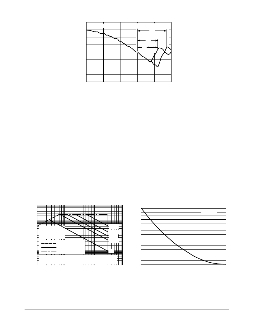
�di/dt = 300 A/� m� s�
�Standard� Cell� Density�
�t� rr�
�High� Cell� Density�
�t� a�
�t� rr�
�t� b�
�t,� TIME�
�Figure� 11.� Reverse� Recovery� Time� (t� rr� )�
�SAFE� OPERATING� AREA�
�The� Forward� Biased� Safe� Operating� Area� curves� define�
�the� maximum� simultaneous� drain?to?source� voltage� and�
�drain� current� that� a� transistor� can� handle� safely� when� it� is�
�forward� biased.� Curves� are� based� upon� maximum� peak�
�junction� temperature� and� a� case� temperature� (T� C� )� of� 25� °� C.�
�Peak� repetitive� pulsed� power� limits� are� determined� by� using�
�the� thermal� response� data� in� conjunction� with� the� procedures�
�discussed� in� AN569,� “Transient� Thermal� Resistance� ?�
�General� Data� and� Its� Use.”�
�Switching� between� the� off?state� and� the� on?state� may�
�traverse� any� load� line� provided� neither� rated� peak� current�
�(I� DM� )� nor� rated� voltage� (V� DSS� )� is� exceeded,� and� that� the�
�transition� time� (t� r� ,� t� f� )� does� not� exceed� 10� m� s.� In� addition� the�
�total� power� averaged� over� a� complete� switching� cycle� must�
�not� exceed� (T� J(MAX)� ?� T� C� )/(R� q� JC� ).�
�A� power� MOSFET� designated� E?FET� can� be� safely� used�
�in� switching� circuits� with� unclamped� inductive� loads.� For�
�100�
�reliable� operation,� the� stored� energy� from� circuit� inductance�
�dissipated� in� the� transistor� while� in� avalanche� must� be� less�
�than� the� rated� limit� and� must� be� adjusted� for� operating�
�conditions� differing� from� those� specified.� Although� industry�
�practice� is� to� rate� in� terms� of� energy,� avalanche� energy�
�capability� is� not� a� constant.� The� energy� rating� decreases�
�non?linearly� with� an� increase� of� peak� current� in� avalanche�
�and� peak� junction� temperature.�
�Although� many� E?FETs� can� withstand� the� stress� of�
�drain?to?source� avalanche� at� currents� up� to� rated� pulsed�
�current� (I� DM� ),� the� energy� rating� is� specified� at� rated�
�continuous� current� (I� D� ),� in� accordance� with� industry�
�custom.� The� energy� rating� must� be� derated� for� temperature�
�as� shown� in� the� accompanying� graph� (Figure� 13).� Maximum�
�energy� at� currents� below� rated� continuous� I� D� can� safely� be�
�assumed� to� equal� the� values� indicated.�
�400�
�350�
�I� D� =� 12� A�
�10�
�300�
�1�
�0.1�
�V� GS� =� 20� V�
�SINGLE� PULSE�
�T� C� =� 25� °� C�
�R� DS(on)� LIMIT�
�THERMAL� LIMIT�
�PACKAGE� LIMIT�
�10� m� s�
�100� m� s�
�1 ms�
�10 ms�
�dc�
�250�
�200�
�150�
�100�
�Mounted� on� 2� ″� sq.� FR4� board� (1� ″� sq.� 2� oz.� Cu� 0.06� ″�
�50�
�0.01�
�thick� single� sided)� with� one� die� operating,� 10s� max.�
�0.1� 1� 10�
�100�
�0�
�25�
�50�
�75�
�100�
�125�
�150�
�V� DS� ,� DRAIN?TO?SOURCE� VOLTAGE� (VOLTS)�
�Figure� 12.� Maximum� Rated� Forward� Biased�
�Safe� Operating� Area�
�T� J� ,� STARTING� JUNCTION� TEMPERATURE� (� °� C)�
�Figure� 13.� Maximum� Avalanche� Energy� versus�
�Starting� Junction� Temperature�
�http://onsemi.com�
�7�
�发布紧急采购,3分钟左右您将得到回复。
相关PDF资料
NTMSD2P102LR2G
MOSFET P-CH 20V 2.3A 8-SOIC
NTMSD3P102R2G
MOSFET P-CH 20V 2.34A 8-SOIC
NTMSD3P303R2G
MOSFET P-CH 30V 2.34A 8-SOIC
NTMSD6N303R2G
MOSFET N-CH 30V 6A 8-SOIC
NTNUS3171PZT5G
MOSFET P-CH 20V 200MA SOT-1123
NTP125N02RG
MOSFET N-CH 24V 15.9A TO220AB
NTP18N06G
MOSFET N-CH 60V 15A TO220AB
NTP18N06LG
MOSFET N-CH 60V 15A TO220AB
相关代理商/技术参数
NTMS7N03R2_05
制造商:ONSEMI 制造商全称:ON Semiconductor 功能描述:Power MOSFET 7 Amps, 30 Volts
NTMS7N03R2G
功能描述:MOSFET 30V 7A N-Channel RoHS:否 制造商:STMicroelectronics 晶体管极性:N-Channel 汲极/源极击穿电压:650 V 闸/源击穿电压:25 V 漏极连续电流:130 A 电阻汲极/源极 RDS(导通):0.014 Ohms 配置:Single 最大工作温度: 安装风格:Through Hole 封装 / 箱体:Max247 封装:Tube
NTMSD2P102LR2
功能描述:MOSFET 20V 3A P-Channel RoHS:否 制造商:STMicroelectronics 晶体管极性:N-Channel 汲极/源极击穿电压:650 V 闸/源击穿电压:25 V 漏极连续电流:130 A 电阻汲极/源极 RDS(导通):0.014 Ohms 配置:Single 最大工作温度: 安装风格:Through Hole 封装 / 箱体:Max247 封装:Tube
NTMSD2P102LR2/D
制造商:未知厂家 制造商全称:未知厂家 功能描述:FETKY?
NTMSD2P102LR2_06
制造商:ONSEMI 制造商全称:ON Semiconductor 功能描述:NTMSD2P102LR2
NTMSD2P102LR2G
功能描述:MOSFET 20V 3A P-Channel RoHS:否 制造商:STMicroelectronics 晶体管极性:N-Channel 汲极/源极击穿电压:650 V 闸/源击穿电压:25 V 漏极连续电流:130 A 电阻汲极/源极 RDS(导通):0.014 Ohms 配置:Single 最大工作温度: 安装风格:Through Hole 封装 / 箱体:Max247 封装:Tube
NTMSD2P102R2
功能描述:MOSFET P-CH 20V 2.3A 8-SOIC RoHS:否 类别:分离式半导体产品 >> FET - 单 系列:- 标准包装:1,000 系列:MESH OVERLAY™ FET 型:MOSFET N 通道,金属氧化物 FET 特点:逻辑电平门 漏极至源极电压(Vdss):200V 电流 - 连续漏极(Id) @ 25° C:18A 开态Rds(最大)@ Id, Vgs @ 25° C:180 毫欧 @ 9A,10V Id 时的 Vgs(th)(最大):4V @ 250µA 闸电荷(Qg) @ Vgs:72nC @ 10V 输入电容 (Ciss) @ Vds:1560pF @ 25V 功率 - 最大:40W 安装类型:通孔 封装/外壳:TO-220-3 整包 供应商设备封装:TO-220FP 包装:管件
NTMSD2P102R2SG
功能描述:MOSFET FETKY 20V.150R LL TR RoHS:否 制造商:STMicroelectronics 晶体管极性:N-Channel 汲极/源极击穿电压:650 V 闸/源击穿电压:25 V 漏极连续电流:130 A 电阻汲极/源极 RDS(导通):0.014 Ohms 配置:Single 最大工作温度: 安装风格:Through Hole 封装 / 箱体:Max247 封装:Tube